ADAU1466 New Board Design Issues
I have made a new ADAU1466 board design that is a clone of the ADAU1466 Eval Board, except for: (1) no codecs (in or out); (2) only uses serial ports in/out; and (3) has a 24.576mhz crystal substituted for the 12.288 mhz. [The new board will be the digital heart of a new audio product.]
I have a clean oscillator signal on the xtal pins (24.576mhz). I have verified all power voltages. The ADAU1466 reset circuit operates normally.
I used Sigma Studio to create, download, and verify operation of a simple design into a ADAU1466 Eval board with the SPI interface (i.e., the USB to 10pin header board, rev. 1.3). The design downloads, operates, and stores in the EEPROM on the Eval board with no problems.
I then set the project hardware configuration registers (using Sigma Studio) so that "PLL CTRL1" = 8, instead of 4 and the Feedback Divider was left at 96. These values were taken from pages 29-30 of the data sheet to set for a 24.576mhz crystal. I then downloaded this version of the project to the ADAU166 on my new board. I verified that the SPI signals are present when downloading the design to the new ADAU1466 Board.
Problem:
1. I do not get any CLK signal out of pin 23.
Question:
1. Other than setting up the PLL and Divider registers, are there any other ADAU1466 registers that would have to be set up differently than for the ADAU1466 Eval board that might be causing the failure to output a CLKOUT signal on pin 23?
Other Issues:
1. I have verified that the "Link, compile, download" menu command works each time it is "clicked on", but I have also verified that F7 seldom, if ever, works. This is a bit noisome, but not significant.
2. Over the years I have spent more time "messing around" with the USB to SPI download cable, drivers, etc. than doing actual engineering work. May I suggest a simple routine and menu item to test the USB to SPI connection. I would be happy to pay real $$$ for this.
3. Is there anywhere to look for a hardware engineer familiar with the ADAU1466 processor? I may have to transfer the remainder of this DSP project to a contractor due to unexpected time issues. I pay competitive hourly rates for qualified engineers.
Thank you!
Patrick
Audio Signal Processors
sigma studio
spi
registers
SigmaDSP Audio Processors
adau1466
Show More
Hello,
Your configuration so far sounds OK to me.
Yes, there is a register for MCLK_OUT that needs to be set properly for a signal to be output. The MCLK_OUT register at 0xF005 should be set to the x8 setting to create a 24.576 MHz output.
I would be curious to know if all your power rails are up and running, and connected to all the pins they should be. In particular, if DVDD is not present it is possible for the XTAL to be oscillating but the core would be unpowered.
On my computer the F7 shortcut has always worked. It's strange that it would be intermittent for you. Are your function keys mapped to system controls by default? If you can provide some more information on your OS version, etc. we can file a report with the programming team.
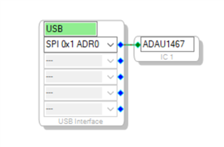
We do have a (limited) mechanism in place to verify the USB to SPI connection; the USB text on the USBi object has a green background when a programmer is present, and red when it is disconnected. We are open to suggestions; what additional features would you like to see here?
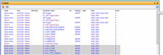
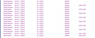
One more thing that may be helpful- are you familiar with the sequence window? It can help us figure out if your DSP is actually active on the SPI interface. You can access it by clicking the << button shown in the top right of the image below.
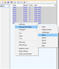
Then, you can select and drag over the clock configuration registers from the capture dialog; remove the delay by highlighting it and pressing "delete"; then,select all the writes and right-click to change them to reads.
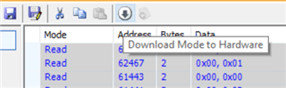
When you press the little download button in the sequence window, the read requests will be sent to the DSP and the results will appear in the capture window.
Then you can see the contents of the registers. If they are all returning 0xFF, 0xFF the hardware is not responding; otherwise the contents of the registers will be there.
Joshua
Joshua,
Very helpful response and I will go through all of it later today. In the meantime, I think I spotted another issue which goes to the question of whether the core is running. I submitted the following to technical support (DSP processors) earlier this morning:
I followed the PLL filter circuit shown in the ADAU1466 data sheet at p. 30 (REV.B) and in the EVAL-ADAU1466Z User Guide (UG-1135), p. 28, schematic for the Eval board. However, I am getting 3.3vdc on the PLL FILTER line (pin 15), not the 1.65 to 2.1vdc specified in the data sheet at pp. 19 & 30. I am not getting a Clkout signal on pin 23. Have there been any issues with this PLL filter circuit? What else could cause 3.3vdc on pin 15?
I have been over my schematic and layout very carefully and I do not see any problems. One difference is that I used an independent 1.2vdc supply rather than the transistor regulator shown in the Eval schematic (I need 1.2vdc for a couple of other low power ICs on the board). I have measured 1.2vdc at each DVDD pin. I have 3.3vdc on all IOVDD pins. The The Exposed Pad on the bottom of the ADAU1466 is soldered to a ground plane. VDRIVE pin is tied to Gnd. Obviously, there is some darn thing I haven't found yet.
Thanks!
Patrick
When my eval board has just been plugged in and no SPI communications are taking place, PLLFILT is 3.3V just like yours. When the PLL registers are enabled and the PLL is running, PLLFILT is 1.99V.
I recommend you probe the SPI interface and verify that programmer data is actually making it to the chip.
I once spent over a week on my own personal board investigating a very similar problem, only to find that I'd populated my 10-pin connector backwards. Lol.
I checked all of my communication pins and here is what I have:
Pin 22 = 0 to 3.3 vdc 24.576 mhz sine wave (very clean)
Pin 23 = Tristate [Clkout (aka MCLK)]
Pin 24 = H (Reset tested ok, active L)
Pin 26 = H (SS_M, connected to SW2, pin 2)
Pin 27 = H (MOSIM, connected to EEPROM pin5)
Pin 28 = Tristate (SCKLM, connected to EEPROM pin 6)
Pin 29 = Tristate (MISOM, connected to EEPROM pin 2)
Pin 30 = Tristate (MISO\SDA, connected to SPI Header pin 5)
Pin 31 = Tristate (SCLK\SCL, connected to SPI header pin 7)
Pin 32 = H (MOSI connected to SPI header pin 8)
Pin 33 = H (~SS connected to SPI header pin 9)
Pin 34 = L (self boot, connected via SW3 to +3.3 for EEPROM)
When I say tristate, I mean neither H or L. My SPI 10 pin header is identical to the SPI header on the Eval Board. I presume that if I get the core working, the pins that are "tristate will become active. I will try the programming again in the morning.
Thanks! Patrick
Joshua,
The only information I have on the pinout of the header cable from the USB adapter board is that shown in AN-1006 which shows a 14 pin header. I matched this up to the 10 pin header shown on the EVAL board by signal function, but it is possible that I did not get this correct. Can you give me a verified pinout from the USB adapter board (matching the actual 10 pin cable from the adapter) so I can re-check the matchup with the 10 pin header on my board. Thank you.
Patrick
Hi Patrick,
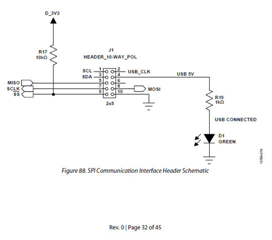
Here is the pinout. It is on Page 32 of the EVAL-ADAU1466Z user guide.
Note that on this board, the SCL, SDA, and USB_CLK lines are not connected.
Joshua
Joshua,
I used this diagram to create my schematic. However, this made me look again at the cabling and it appears that I made the exact same mistake as you did with reversing the header layout. Let me list the color code of the wires from the USB adapter just to make sure there is no more confusion:
Brown = Pin 1 = SCL (not used)
Red = Pin 2 = USB CLK (not used)
Orange = Pin3 = SDA (not used)
Yellow = Pin 4 = USB 5vdc (to green LED)
Green = Pin 5 = MISO
Blue = Pin 6 = NC
Purple = Pin 7 = SCLK
Grey = Pin 8 = MOSI
White = Pin 9 = ~SS
Black = Pin 10 = Gnd
So, it appears that my schematic, netlist, and layout were correct, but the header on my board is reversed with respect to the ribbon cable from the USB adapter. That will be a simple fix. I am a little concerned about the 5vdc I may have put onto my SCLK line, but I just checked with my scope and the voltage floats gently to 5vdc, so I may be lucky and not have damaged this pin. I will let you know if this gets the SPI operational.
Thank you, Patrick
Hi Patrick,
That's pretty funny that we might have made the same mistake! It's a very easy one to make. Some headers have little embossed arrows pointing to Pin 1 to help you out. Mine didn't.
I highly recommend labeling this board so you don't mix it up with another one. Now that it's had 5V on a signal line it should be classified as a test board.
Joshua
Joshua,
Good news! My ADAU1466 verified fully operational, plus EEPROM circuit verified and I am able to download and boot from code. All signals look good, so it is onward to some operational testing. Its great to make a Rev. 1 board and not have any cuts/jumpers -- just a darn header cable mixup.
Thank you for your patient help.
Patrick
Please log in to reply.