Table of Contents
Flash Programmer (ADAU145x)
This module provides support to write raw data to the external flash memory using I2C/SPI. The I2C/SPI write is performed during the initialization before the audio processing in the schematic is started.
Configurations
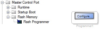
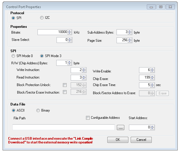
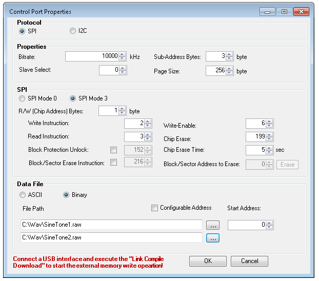
Click on the configure button to configure the SPI/I2C interface for the module.
| GUI Control Name | Default Value | Range | Function Description |
|---|---|---|---|
| Protocol | SPI | SPI/I2C | Master Control Port Protocol |
| Bit Rate | 100kHZ | 100 kHZ - 100000 kHZ (for SPI)/ 400 or 800 or 1000 kHz (for I2C) | SPI/I2C Speed |
| Slave Select | 0 | 0-6 | Slave Select for the SPI. Register window should be configured to match this selection.Please refer the note below. |
| Sub-Address Bytes | 2 | 1-4 | Number of address bytes excluding the read/write command |
| PageSize | 128KB | 0-32MB | Page Size of Flash |
| SPI Mode | Mode 3 | Mode0/Mode3 | SPI operation mode |
| R/W (Chip Address) Bytes | 1 | 0-255 | Command Bytes (Number of bytes required for command) |
| Write Instruction (SPI) | 2 | 0-255 | Instruction value for a write operation (0x0 for ADI audio devices, typically 0x2 for eeprom/flash) |
| Read Instruction (SPI) | 3 | 0-255 | Instruction value for a read operation (0x1 for ADI audio devices, typically 0x3 for eeprom/flash) |
| Write-Enable instruction (SPI) | 6 | 0-255 | Instruction value for device write-enable operation |
| Block Protection Unlock (SPI) | 152 | 0-255 | Block Protection Unlock command for SPI falsh devices. This is an optional command. This can be disabled. |
| Chip-Erase instruction (SPI) | 96 | 0-255 | Instruction value for device erase operation |
| Chip-Erase Time (SPI) | 5 sec | 1-600 sec | Time required for chip erase operation |
| Block/Sector Ersae Insutruction (SPI) | 216 | 0-255 | Block/Sector erase command for SPI falsh devices. This is an optional command. This can be disabled. |
| Block/Sector Address to Ersae (SPI) | 0 | 0-16777215 | Block/Sector address to erase SPI falsh devices by block/section. This is an optional command. This can be disabled by disabling the Block/Sector Ersae Insutruction |
| Data File | NA | NA | Raw data to be written to the flash (Can be ascii text file/ binary files like wav file) |
| Data File Mode | ASCII | ASCII/Binary | Mode to write the file. Audio files like .wav should be written in binary mode |
| Configurable Address | Disabled | Enable/Disable | Enable/Disable the start address for each files |
| Start Address | 0 | 0 - Maximum of FLASH/EEPROM Size in bytes(Increment by page size) | Write the data in the flash/e2prom from the specified address |
Any change in these SPI/I2C configuration parameters requires a recompilation.
Note:
The following image shows an example ASCII data file.
- ding.txt
[ASCII 44100Hz, Channels: 2, Samples: 5, Flags: 0]
-0.005768
-0.005768
-0.003235
-0.003235
-0.002167
-0.002167
-0.004151
-0.004151
-0.005554
-0.005554
Writing Multiple Files
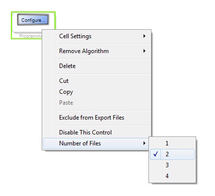
Number of files to be written can be configured by right clicking on the module. All the files will be written one after another if multiple files are selected. This support upto 32 files.
Example
Writing a Wav file to SPI EEPROM using Flash Programmer (ADAU1452)
- Add Flash Programmer module to the schematic.
- Configure SPI parameters in the Control Port Properties window. (Below window shows SPI configuration required to write to EEPROM in EVAL-ADAU1452MINIZ board)
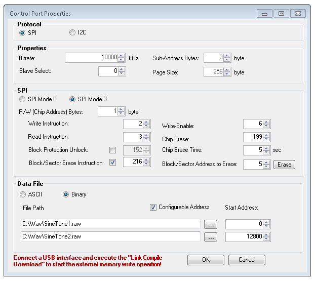
- Select Binary mode
- Select the Wav file to be written (Make sure size of the wav file is not greater than the size of EEPROM. In the case of EVAL-ADAU1452MINIZ, size of wav file should not be greater than 128 KB)
- Press OK. Then Link compile download.
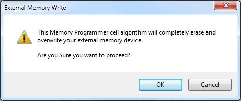
- Press OK when the following warning displayed.
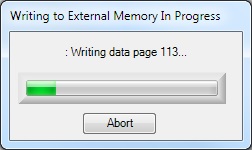
- Then the wav file is written to the EEPROM.
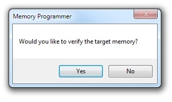
- After the write is completed, press Yes in the following window to verify the write operation.
- Verification should be successful as shown below.
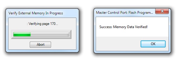
- Verification will fail if the file is more than 128 KBytes. Make sure file is not more than 128 KBytes and re-write if it is failed.