ADAU1463/1467 SDATA IO settings
Hello Dave,
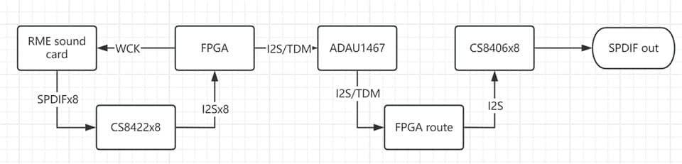
Here is the audio path. FPGA will output word clock to RME sound card to align the output clock with FPGA clock. so no matter RME is slave or master, FPGA will be the master.
attached is the project file. please note that I don't use PLL inside of the chip, cause I have external reference OCXO as the source.
ADAU1467.V0.1.dspproj
I need to use 8 ASRC to unify the input signal to 96K sample-rate and do processing using PEQ, etc.
my question is if I don't use TDM as data bus, could I use 4 SDATA IO as input and 4 SDATA IO as output? and how to set this up.
if this project works well, I'll later put more into the board like ARM64, and make it a special audio snap circuit, cause I figured out that the most needed audio requirement is like this. simulation or correction...
Best regards,
Power Pan
Edit Notes
typo
[edited by: PowerPan at 11:44 AM (GMT -5) on 10 Jan 2025]
Audio Signal Processors
software
sigmaStudio 4.7
adau1467
SigmaDSP Audio Processors
Hello Powerpan,
I can see that, Dave has been supporting you in this case and there is no better person than him.
I just wanted to share some of the details and a project for 8 I2S input and 8 I2S output by using the SDATAIOx pins of ADAU1467. I hope your sample rate is 48KHz. This is important because at 192KHz, there is a bug with the SDATAIO pins in the input side. I have attached that thread as well here
PowerPan said:
my question is if I don't use TDM as data bus, could I use 4 SDATA IO as input and 4 SDATA IO as output? and how to set this up.
So, we have four input and four output ports. Hence, we have four primary I2S inputs and four primary I2S outputs (one I2S for each input and output port). For the rest four I2S inputs and I2S outputs we are going to use the eight SDATAIO pins.
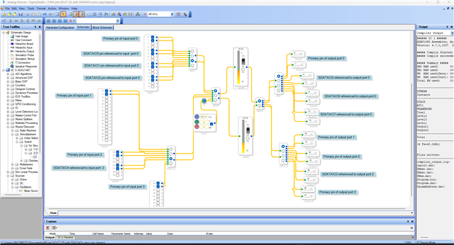
Please find the project below where I configured 8 I2S inputs and outputs. I put comments in the schematic for better understanding.
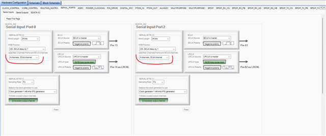
IMPORTANT: There is a bug with SDATAIO pins when using it in the input side that is, we have to set the SDATAIO pin using input port as TDM4 like below. If the serial input port is the master, then set it like below.
If the serial input port is slave, then send TDM4 clock (which typically is 6.144MHz at 48KHz) from the serial clock source. If you have any problem with this setting of TDM4, then there is a workaround given this thread, please check here. You can follow which is suitable for your application.
Below is the screenshot of my project.
4IN and 4OUT I2S with SDATAIOx pins copy.dspproj
Here is the project for 16 channels IN and OUT (as 8 I2S in and 8 I2S out)
I hope it will be helpful.
Kindly follow Dave's advice from here.
Regards,
Harish
Hello PowerPan,
Thanks Harish for the example schematic. You detailed the bugs well and it is a tricky thing to use the SDATAIO pins but they are a great capability.
Thanks PowerPan for the diagram. It is SO SUPER helpful!! It looks like you have the FPGA handling the accumulation of the data and the interface and clocking. So I would simplify the SigmaDSP part of this a lot!! If you try to use only I2S then you will have to go to two chips. If you use the FPGA to combine the stereo audio into TDM-4 streams then you can do this with only one chip and keep the bit clock speeds down to a lower frequency to allow for better timing margins for the data transmission. This is important when operating as a clock slave. Look at the timing diagrams for the tSODS in table 9 of the ADAU1452 Rev D datasheet. I added the timing based on the pin drive strength so if you study this you will see that you will have to setup the pins for a higher drive strength to make this work. Either setting 0b10 or 0b11 will be fine. There is little difference between those settings. This will be for the SDATA pins that are an output. The serial output pins. I had added all these to the datasheet back in 2018 and the ADAU1467 was never updated but these parts are so similar that it will apply to the 1467.
So if you setup this board to use four TDM-4 data lines in and out then at 96kHz sampling rate you will have a bit clock rate of 12.288MHz which will give you around 40ns for the data to settle. If you increase the drive strength then you lose only 9ns for the data to come out of the part. This will leave time for the round trip of the signals between the part. Sorry, I am keeping this short but I suggest you set this all up for TDM-4 and it will make life easier for you down the road! Then you can do this with one part!
Thans for mentioning the PLL. you absolutely MUST, and I mean MUST use the PLL. If you do not then the MCLK input will be the internal system clock. You did not mention what the OCVO clock frequency is but I am guessing it will be 12.288MHz? So this is what you will get.
The system clock goes to the clock generators. So 12.288MHz gets divided by 1024 and then your settings for clock gen1 is an N/M of 1/6 which means you further divide this by 6. Your base sampling rate will be 2.096kHz. Yes, 2kHz. I do not think this is what you want.
You have to increase the internal system clock up to 294.912MHz. then when you do all the dividing you will get the base rate of 48kHz.
Using a clean clock for the MCLK input is really good. Using the PLL will not increase the jitter. It will actually help reduce it.
By the way, to continue looking at your project. You set the SigmaStudio sampling rate to 96kHz but that does NOT set the core sampling rate. That is all done with register settings and ultimately the clocks you are feeding to the part. You did not give the frequency so I am a bit stuck but I will assume it is 12.288MHz.
You also had nothing for troubleshooting and verifying things like correct channels in correct places and correct levels etc. So I built a project for you.
This was based on a project I had showing how to use all 48 inputs and outputs. So this one just uses 16 inputs and outputs.
I split it up in boards to make it simpler on the screen.
You have some meters to switch between input ports so you can see if anything is getting into the core.
Then I have an oscillator you can select on the output side to output a known level.
There are mutes for each channel so you can mute one channel and verify it is indeed the channel you think it is.
I also set it up for 96kHz.
Since it looks like you will be using the same master clock for the FPGA and the SigmaDSP then you will not need the ASRC but!! and this is a big but!! It will follow the sampling rate out of the PFGA, However, If you do change to 48kHz then the frequency curves on the EQs will be wrong.
So in the end I think you may have to use the ASRCs. You could add some switches to the input to change it to bring in the ASRCs. However, I am just realizing that the output will still not be correct. The part only has 16 channels of sample rate conversion. So you can convert the input or the output but not both with only one chip.
Gee, this might need some rethinking... I setup the DSP start pulse to use the sampling rate of the serial input port 0. So it will follow what it is being sent from the FPGA. If you have an EQ that is set to 20kHz LPF for instance. With the filter calculated for 96kHz it will work fine at 96kHz but if you change to 48kHz then it will be a corner frequency of 10kHz. It will be the same percentage of the sampling rate but the absolute number will be different. This is no huge deal when going from like 48kHz to 44.1kHz. The frequency is slightly off but not huge.
How to solve these issues is tough. I do not know the full big picture of what you want to do. The real problem here is the EQ and the delays. Those all change with sampling rate.
You can put in different EQs and delays for different sample rates and have the program check the ASRC ratio and switch if the sampling rate changes but I just checked and this project compiles and uses 124% of the available cycles!!
This means this program will not run at 96kHz already! I looked at what was using all the cycles and most of it is the PEQ.
Well, I guess this is telling us you will have to use two chips. eight channels per chip. This way you can use the sample rate converter going into and out of the part. You should be able to bypass them if they are not needed but that is another post. I have posted examples of that a long time ago.
By the way, by going to two chips then you can just run each serial port in I2S mode for two channels each and have no issues with timing!
Here is the project I worked on.
Dave T
ADAU1467 16 in and 16 out using all TDM4-I2C.dspproj
Hello Dave and Harish
Thanks for your prompt and kind help with my project. I am on a business trip and will be back Monday night. I will have a look then.
I always use 24.576/49.152MHz as the MCK for the DAC/class AMP. Note that the PLL is a must for the system core.
ASRC is for different sample rate signals to be mixed later on. So 8 stereo sources might have 8 different sample rates so I need the ASRC. and output could be the same sample rate.
if 2 chips are a must I'd rather use 2 adau1452 instead cause 1452 is more common with almost the same resources as 1467.
I'll consider to modify the circuit later on.
Power Pan
Please log in to reply.