Level Discrepancy between 1701 to 1467
Hi, I am working through some issues on interface of a 14/1701 with the EVAL ADAU1467. I have the 1701 sending serial audio over Serial Input Port 3. I notice there is about a 3db loss of audio coming from the 1701. I have a gain block in the 1701 to compensate, but I also noticed the datasheet shows this is a 28 bit resolution verses the 1467/1937 which deals with 24 bit resolution. Does this perhaps have something to do with the level discrepancy or are there hardware differences in the A/D that account for this. Thanks!
Thread Notes
ElsaDog - Moved from SigmaDSP Processors & SigmaStudio Dev. Tool to Processors & DSP. Post date updated from Wednesday, March 4, 2026 5:18 AM UTC to Friday, March 13, 2026 5:53 PM UTC to reflect the move.
Audio Signal Processors
software
4.7
adau1467
processors and dsp
SigmaDSP Audio Processors
Processors and Microcontrollers
adau1701
Show More
Hello ElsaDog,
There are a few little things not correct in your statement but I think this could be a serial port setting but I am not sure.
The ADAU1701 has an internal number format that is 28 bits. It is setup as 5.23.
Here is an excerpt from the datasheet:
"The input and output word lengths of the DSP core are 24 bits. Four extra headroom bits are used in the processor to allow internal gains of up to 24 dB without clipping. Additional gains can be achieved by initially scaling down the input signal in the DSP signal flow."
There are four bits of headroom. So the 1.23 is the audio in and out with the "1" being the sign bit. It is 24 bits of data. So we add four bits for 24bit data coming in and only use the bottom 24 bits to go out.
So if you place a meter in your project and set you see 0dB then you have a 0dBFS 24 bit signal. The easiest way to verify this is with an oscillator block. The oscillator blocks will put out EXACTLY 0dB 24bit signal. Send that out of the serial port and it will be a full scale 24 bit signal. Take that into the ADAU1452 and it will show up as a 0dB signal in that core provided the serial port settings are correct. Use an oscillator block, send it out and then when it comes into the other DSP send it directly to a meter and see what you read.
The ADAU1452 is a very different core. It is a 32 bit core. However, we did set it up for the default of 24 bit in and out of the core. We take the 24 bits coming in from the serial ports and add one bit to the bottom of the 24 bits and seven bits to the top to give it 42dB of headroom.
So the internal format is 8.24 which is 32 bits.
So when we send out the data, we truncate the bottom bit of the 32 bits and then send out the bottom 24 bits of that 31 bit signal therefore chopping off anything above the 1.23 signal.
So we chop it the bottom making it an 8.23 and then shop off the top 7 making it a 1.23 signal.
Again, the meters in the core are setup for this. Set the meter in SigmaStudio for 0dB and you will see a 0dB signal if it is a 24 bit signal positioned in the 1.23 data position.
Now, each bit is ~6dB. This is digital theory. 6.02dB per bit. A shifting or loss of one bit will cause a roughly 6dB difference. If you are only seeing 3dB then this is simply a gain setting somewhere.
Just do as I suggested with an oscillator and a meter and check your serial port settings to make sure they are both setup correctly.
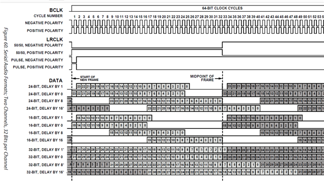
Page 66 of the ADAU1452 datasheet details the bit locations in the serial stream. Hook up a scope and check it.
I wrote this post a long time ago on how to take screenshots if you need some pointers.
(+) How to Take Meaningful Screenshots of I2S Audio Signals - Q&A - Audio - EngineerZone
Basically, I am saying that there should be no discrepancy between the two if you use the 24 bit defaults and setup the serial ports the same and have the same level measured in the core with a meter.
Dave T
Ok, that makes sense. If I could just impose on one more question, for now. I have a single level detect monitoring the input from the 1701. With no input to the 1701, my level indicators in the 1467 are showing a constant -34dbm. I am routing this signal externally to output pins and see nothing on the output on a scope. The level is constant with zero variability in that reading. I have the 1701 in slave, the 1467 in master, there are no clock slips that i can see, and the port are both configured tor I2S. I am thinking this is some artifact, but cannot see where it is being generated. When I disconnect the serial stream from the 1701, it disappears, so it is either being generated by the 1701, or is some kind of interpretation error in the signal. Do you have any ideas where I might start? Included both programs for reference. Thanks!4162.Audio Input 1701 Board 03072026 Serial Input 0 DIG2 DIG3.dspproj6153.Controller Audio Squelch PL MIX w1701 v 1.3 03062026.dspproj
Hello ElsaDog,
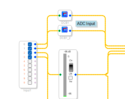
Sorry it has been a busy day and I have not been able to download your projects. One quick question. Did you place a DC block on the ADC outputs of the ADAU1701? The converters, all ADC converters, have a DC offset. Most converters have a register setting to add a HPF but this part does not. I guess the designers thought that hey! There is a DSP core, just do it there!
I would have advised them otherwise, but I was not working here at the time!
This is what I do with all my ADAU1701 projects:
Dave T
Added a 10Hz Hi pass and discovered this, so your DCblock is much more elegant and added to the project. I am getting some very small clicks that sound like clock or frame slips on serial input 0 from one of my 1701s. If you would not mind taking a look at my register settings in both to see if anything obvious, I would greatly appreciate it! Thanks!
Hello ElsaDog,
I did download your projects. It looks like you are sending I2S out of the 1701 and into the 1467 and it is at 48kHz fs. Does that all sound good?
Clicks can happen a few different ways making this a bit tough for me to figure out from here. So I will mention a few things to check and some possible causes of a problem like this.
1) Is the master clock for the 1467 and the 1701 coming from the same place or are you sending the CLKOUT of the 1467 to the 1701 master clock input. If they are on their own crystals then they can never be exactly in sync and errors can pop up from time to time. I do not expect this to be the issue. I am guessing you have this part done correctly but I needed to mention it. Plus, others can read these posts!!
These next two reasons combined is probably what is the cause of what you are describing.
2) The serial output port is set to slave to the external clocks... When you set the clock direction opposite of the data direction, you have the issue where the incoming bit clock edge has to be detected internally as the edge. Then internally it "says" "Oh! here is the edge, what is the next bit? Get it and send it to the data output pin! " I am acting like it has a brain but what it has to do is grab the next bit and put it out of the data pin which takes time!! This time is detailed in the specifications as tSODS. Which for this part is 40ns. Soi for a 3.072MHz bit clock, (48kFS times 64 bits in a sample period for I2S) This means one clock period is around 325ns. For I2S at 48kHz it is not too bad but for TDM 16 it would be 40ns for one block period!!
However, I need to detail this further. The Bit clock edge comes out of the clock pin and has to travel to the DSP. This takes time!! Then what I described above with the delay to present the data to the output pin is another delay. Then the data has to travel back to the serial port of the other device! So this round trip has to happen before the other edge of the bit clock happens which will clock in the data. If it is late then you have a bit error which can often be heard as a click or pop.
3) Signal integrity and PCB layout. If the traces are long then it takes more time for the clock edge to get there. If there is a lot of stray capacitance then the rise time will be delayed. If there is too much drive strength and little to no damping then there may be a strong reflection which will cancel out the signal shortly after the edge which can mess up the detection of the edge. Signal Integrity is a huge subject but it is part of this where it involves the travelling of the clock edge from one part to the other.
Looking at this closely on a scope is important and may allow you to see a possible cause or a clue.
I did write a post many years ago about taking screenshots and looking at I2S signals.
(+) How to Take Meaningful Screenshots of I2S Audio Signals - Q&A - Audio - EngineerZone
Enough for now!
Dave T
Hi, Dave!
On Point #1, The Master Slave language is a bit ambiguous for me, so perhaps you can clarify. The output registers in the 1467 appear to be set to out, master (I have tried different options lick slave from domaine 0) but the BCLK and LRCLK is master only seems to pass audio. So I would have assumed that the input to the 1701 would be the BCLK and LRCLK input on pins MP4 and 5, but those do not respond to the 1467 clock, so they are on MP 10/11. (L on 4/10 and B on 5/11) So even tho 10/11 seem to suggest they are ouput lines, that is the connection, and it works on the other identically configured board. The only check box I see for master operation is in the Serial Output box on the 1701 register page. It is not checked on either board.
Ah, so on point 2, are you then suggesting that we use the 1701 as master to avoid the round trip delay? What settings would I select in the 1467 to allow the 1701 to act as master?
I will connect a scope later to see if I am rounding the edges, and this is certainly possible as we are not dealing with traces, but wire connections between the 1701 and 1467 eval board. I am a bit perplexed about this being the cause, however, as the other 1701 is not exhibiting this behavior. Since I have exactly the same setup, interconnect method, schematic and register settings on both boards, I keep coming back to something being off in the 1467 between Serial Port 0 and 3, but I sure cannot detect it.
Thanks for your help, hope this triggers something in your experience.
Cheers, ElsaDog/Chuck
Hello ElsaDog/Chuck,
Let me start with the Master/Slave language. Just to be clear and I think you are not confused with this but when a serial port is a master, it will supply the clocks to the other external device. If it is s slave, then it is an input for clocks that will be supplied by some external device.
The ADAU1701 only has one serial port. So usually in this case you have only one selection. either it supplies the clocks (a master) or it is accepting and external clock (a slave).
To either clock in or clock out a bit, you need a clock pulse (edge) to do that! Yup, makes sense. Usually how a chip is designed there is an internal "Y" connection between the serial data out and the serial data in. So there is only one set of clock pins. If the clock is coming from external it is "Y'd" and sent to both shift registers for the data input and data output. If the clock is coming from an internal source, then the clock of course goes out of the clock pins but also goes to the internal shift registers.
Here is where the designers of this part did something strange. They brought out the clocks for the two shift registers out to their own pins and did NOT connect them internally!! If I were here I would have advised them otherwise.
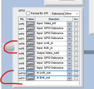
So here are the MP pin assignments. By the way, to make things worse they even named the pins in a strange way!
MP4 and MP5 are the clock pins for the serial DATA INPUT shift register. These are ALWAYS a slave and always need to have a clock feeding into these pins if you want to accept data into the serial port. If you do not want to receive data then you do not need to clock these pins.
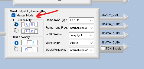
MP10 and MP11 are the clock pins for the serial DATA OUTPUT port! These pins can either accept clocks, (a slave) or can produce clocks (a master). There is a register setting for this and here is where you select it in SigmaStudio:
So the DSP is the clock master and if you need to clock in serial data you have to externally jumper MP4 over to MP10 and MP5 over to MP11
For your next question:
ElsaDog said:
Ah, so on point 2, are you then suggesting that we use the 1701 as master to avoid the round trip delay? What settings would I select in the 1467 to allow the 1701 to act as master?
Yes, this is what I suggested without knowing anything else about your system. I was assuming you were using an external set of ADCs or DACs etc. Since you are sending to another DSP I really would need to see the clocking and data flow of the entire system. These things can get a little tricky and sometimes it is all about tradeoffs.
Next, if you are connecting with wire jumpers then I am super concerned. This is not good for signal integrity. The signal return currents are not clearly defined. If I use jumpers I will either twist a ground wire along with it or run ribbon cable with ground alternating with signals on the ribbon. This certainly can be the source of the data errors.
This again ends up being such a big subject and I cannot write a book in a post! LOL
Dave T
Thanks, Dave. Yeah, I get the clock functionality, I was just confused by the pinout naming convention. Now that I understand there is sep clocking for input and output, the naming makes more sense.
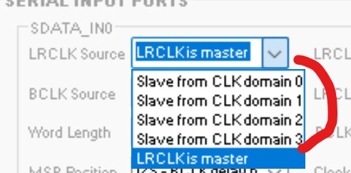
When I set the 1701 as master, what is the corresponding setting on the serial port clocking options for 1467? I think it gives the option to select from one of the four serial input streams, (it references "domain" another introduction of terminology)but not readily apparent from the nomenclature.
Lastly, the DSP 1467 eval board provides header pins for external data and clock, so I have to believe they expected connection using some kind of wiring to deliver this signal. I used to design grounding, bonding and shielding techniques in telecom, so I will try your isolation and ground techniques should they be necessary after I change the source clocking, but, again, the other is working fine, which could be a function of different capacitance on one port vs the other.
Very good information, if you could clear up the settings on the 1467, that would be appreciated!
Thanks again!
Chuck/Elsadog
Dave:
First, I want to thank you for your time and detailed explanations of the functionality of these devices! Of course, we could just read the #$% documentation and figure this out, but your experience is a fantastic resource that makes it easier, and me lazier! (are you AI?)
Okay, so I re-read your answer to #2 and this, of course, made perfect sense when considering the clock frequencies involved. It looks like they even give you some options to set the clock to lower speed if your application can tolerate it to help mitigate some of that effect, but be that as it may, I switched to master on the 1701 and presto! Problem solved! This issue was very subtle, and many would not notice it, so I am guessing there must be a bit of a tolerance variance in the way the other serial port is routed/capacitance that makes it more tolerant of the misinterpretation of the clock edge.
So, I have configured both 1701s to master and aligned the slave in the 1467 to track to the input port which I assume is "domain" as as soon as I selected it, it all came up running perfectly.
Thanks again for your patience and detailed descriptions of the behavior of this incredible hardware. I have ever increased plans on how to leverage this stuff. I just ordered another EVAL1467 for another project as I could not be more impressed with its capabilities.
Cheers!
Chuck/Elsadog
Hello Chuck,
Sorry for the delay in my response. Been kind of crazy around here!!!
You ask is I am AI? I am,... Admittedly Insane!!
You sort of have to be when it comes to working in the audio world!
OK, Enough horrible humor. Good thing I am not quitting my day-job!
OK, I it seems like you understand the clock pins on the 1701.
For the ADAU1452 and ADAU1467 family of parts are a very different setup for the clocks.
It is not too difficult once the basic understanding is there. I suggest you download the ADAU1452 Rev D datasheet. I had put in a lot of effort revising and adding information to that revision back in 2018. These revisions never made it to the ADAU1467 family of parts and many of the details apply to both families. Clocking is certainly one of them.
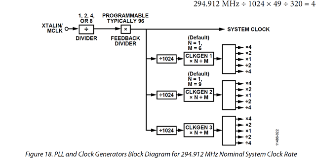
Here is an important diagram for the internally generated clocks.
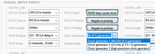
So when you have register settings to select internal clocks you have choices of which clock generator and then which output of the selected generator.
So you have two registers to choose the correct intended clock:
The first is which of the three clock generators do you want? 1,2, or 3?
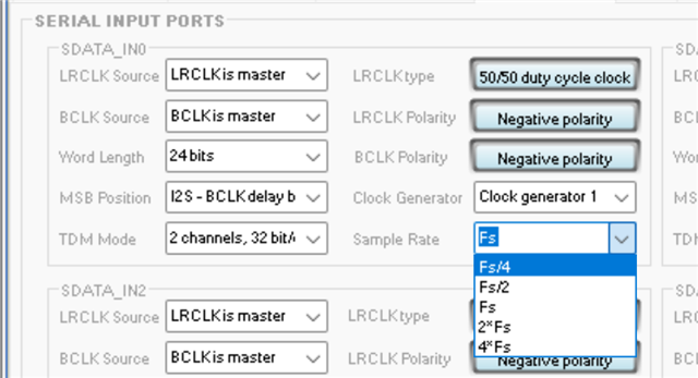
Then you choose which output of the selected clock generator do you want to use?
Note it says divided by 4 or 2
Then X1
Then multiplied by 2 or 4 like the clock generator diagram shows that I pasted up above...
So that handles when you use internal clock sources as the master.
OK, now on to when you have the serial ports as a clock slave....
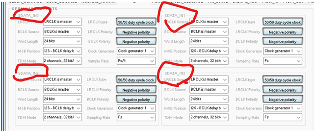
There are four sets of clocks (LRCLK and BCLK) for each serial INPUT port.
These are labeled serial ports 0-3
So each has their own set of clock pins.
However, these four sets of pins are buffered and distributed so ANY of the serial input ports can use that set of clocks!! So if you are using all four serial ports from a part on the same clock domain then you only need to connect the clocks up to one set of pins and use the internal distribution buss to buss it to the other three serial inputs. This is where the "slave from domain" settings are for.
So EACH serial input port can slave from any other serial input port's clocks.
Now here is where there is a wrench in the works....
The serial input ports and output ports are not connected together in any way!!! Yes, you can choose the same internal clock source, But when slaving, you cannot slave an input port from an output port as one example. The other way applies as well. There is no internal buss between the inputs and output clock pins.
There are four sets of clocks for each serial OUTPUT port.
So Input clock domain 0 is NOT the same as Output clock domain 0.
If you need them to be then you MUST externally connect the LRCLK and BCLK from some external source to one set of input pins and one set of output pins.
This gives you so much flexibility for clocking but it is a little confusing at first.
I hope this helps...
Dave T
Please log in to reply.